Trends
Packing technologies have made for cuts in both the geometry and weight of telecommunication devices. We are still evolving to achieve even a larger scale of integration.
We have been producing packages since 1981. The compact packages we produce have been extensively used in cell phones and other compact portable devices. Keeping pace with the growing complexities of device functionality, we have been working on downsizing our products more, while reducing their cost and enhancing their performance.
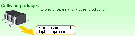
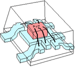
While gullwing packages now in widespread use are surface-mounted with the tips of leads bent outward, flatlead packages have come into being to meet the demand for higher scale integration amid the mounting needs for lower profiles and smaller geometry.
Flatlead packages suppress variations in lead forming because they do not involve lead bending, and allow more chips to be mounted in the same mounting area.
The characteristic of the flat lead package
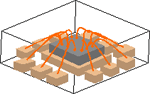
The characteristic of the lead less package
Page Top