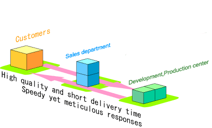
About Our Service
1. Package assemblies
We implement it and deliver it to an external form desired if we have you provide it with a semiconductor wafer. It processes it and copes with an individual process as well as coherent work from a die thing to a test, packing.
2. Wafer processing
Back grinding
We are able to back-grinding to the thickness of 100μm for wafer of 150-200mm in the diameter without the crack and the dividing.
- Optimization of grinding condition
- Condition putting out matched to process of wafer
- Analysis tecnology of damage
Dicing
We are able to back-grinding to the thickness of 100μm for wafer of 100-200mm in the diameter without the crack and the peeling. It is possible to correspond.
- Optimization of dicing blade
- Optimization of dicing condition
- Optimization of dicing tape
3. Test Service
We provide you with best test solutions by making full use of technological prowess and know-how specific to manufactures specializing in semiconductors and the latest-type testers.
Contents of Service
- Test engineering support
- Development and debugging of test programs.
- Design and making of test boards and fixtures.
- Information provision service
- Test result summary information
- Production control achievement information
4. Diverse package variations
Our packages, available in diverse variations, enable us to fulfill whatever requirements you may have for packages, from small IC packages to transistor super-compact packages. Among other things, we have an abundant supply of discrete system packages.
5. Environment responses
We have been working on a program to make the solder used in lead processing lead-free. (For a detailed schedule, contact.)
Page Top